

DSP Educational Vehicle & iCE40 Mixed-Signal Laboratory
The Pico Dev-iCE is a low-cost, high-performance "Lab-in-a-Box." It combines the high-speed programmable logic of a Lattice iCE40UP5K FPGA with the flexible C/MicroPython ecosystem of a Raspberry Pi Pico (YD-RP2040 with 16MB Flash).
Designed specifically as an educational platform, it abandons "black box" RF chips in favor of discrete, observable analog blocks. Students can physically probe the RF signal path, design their own LC filters on pluggable sandboxes, and write Verilog to perform Direct Digital Conversion (DDC), digital decimation, and hardware I2S audio routing.

Here is a video of the SDR receiving on 20 meters.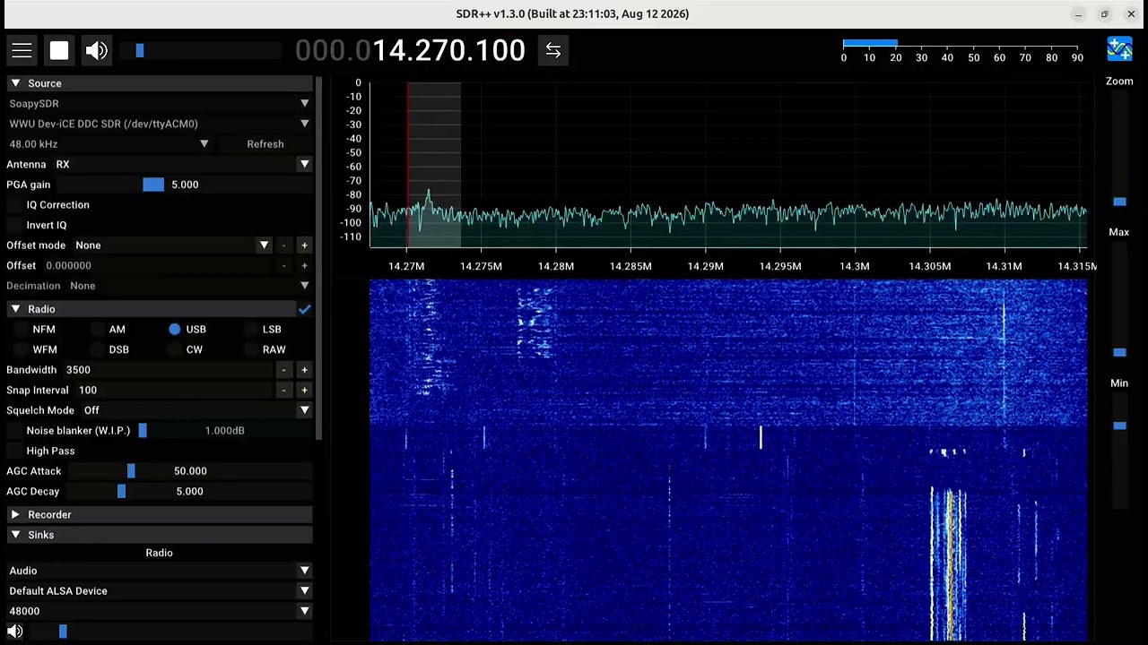
- HF Software Defined Radio (RX/TX): Full-duplex DDC/DUC transceiver covering 0 - 15.36 MHz (1st Nyquist) with Super-Nyquist capabilities up to 30+ MHz.
- Vector Network Analyzer (VNA): Built-in Return Loss Bridge (RLB) for S11 (reflection) antenna tuning, and Port-to-Port S21 (transmission) filter characterization.
- Arbitrary Waveform Generator (AWG): Dedicated DC-coupled and AC-coupled SMA outputs for 30 MSPS generic signal generation.
- Real-Time Spectrum Analyzer: Visualize the entire 15 MHz HF spectrum simultaneously via FPGA-accelerated FFTs.
- Standalone Operation: Onboard Audio DAC/Headphone amp and rotary encoder support allows the board to operate as a standalone radio without a PC.
- Microcontroller: YD-RP2040 / Pico 2 socket. Handles AGC math, user interface, USB communications, and slow-state hardware toggles. The massive internal Flash (up to 16MB) stores the FPGA bitstream and programs the FPGA directly on every boot, eliminating the need for an external FPGA flash chip.
- FPGA: Lattice iCE40UP5K (SG48). Handles high-speed 30.72 MHz DSP, NCO generation, CIC decimation/interpolation, and I2S master clocking.
- Control Bus: The Pico uses its high-speed
SPI0bus to dual-role: it blasts the bitstream into the FPGA's internal CRAM on boot, and then seamlessly transitions to sending runtime DSP commands to the user's Verilog over the exact same 4 wires.
- Master Clock: A clean 30.720 MHz CMOS oscillator drives the FPGA.
-
The Magic of 30.72 MHz: The FPGA decimates the 30.72 MSPS ADC data by exactly
$R=640$ to yield a mathematically perfect 48.000 kHz baseband I/Q audio stream over I2S to the Pico. - Process Gain: The 640x decimation provides ~ 28 dB of digital processing gain, turning the raw 8-bit ADC into a highly sensitive 12.6-bit effective receiver!
- Topology:
SMA➔Ethernet Isolation/CMC➔Band Sandbox➔T/R Switch➔LNA 1➔PGA (5/10dB)➔LNA 2➔ADC. - Amplifiers: Uses discrete high-speed op-amps wired as AC-coupled inverting amplifiers.
- Programmable Gain: A Digital Step Attenuator (DSA) built from CMOS switches and precision T-networks, providing 0 to 55 dB of gain control in 5 dB steps. LNA 1 and LNA 2 are both bypassable to prevent clipping on massive signals.
- ADC (MS9280): 8-bit, 32 MSPS. Driven by an RF balun into True Differential Mode with a 4.5V analog supply, yielding a massive 4.0V peak-to-peak input span for maximum dynamic range.
- Topology:
DAC➔Passive I-V➔Ethernet Transformer➔TX Switch➔Recon Sandbox➔TX Op-Amp (+12dB)➔T/R Switch➔SMA. - DAC (MS9708): 8-bit, 32 MSPS Current-Steering DAC.
- Passive 50Ω resistors and an Ethernet transformer gracefully map the DAC's strict output compliance limits into a clean 1.0V p-p RF signal, which is then amplified to drive a 50-ohm antenna.
To achieve commercial-grade noise floors, the noisy Switch-Mode Power Supply (SMPS) of standard Picos is bypassed/isolated.
+4.5V AVDD: Clean LDO powering the RF op-amps, analog switches, and ADC/DAC analog cores.+3.3V Digital: LDO powering the FPGA I/O, Pico, and IC logic.+3.3V Clean: Ferrite bead + LC filtered rail strictly for the 30.72 MHz oscillator to eliminate phase-noise/jitter.
SDR_ANT(BNC): Main Transceiver Port (Transformer isolated, AC-Coupled).SII(SMA): Device Under Test port for S11/VSWR Antenna measurements. Connects to the internal Return Loss Bridge.AWG_OUT(BNC): Direct DC-coupled output (0V to +4V) from the DAC. Perfect for baseband signal generation.S21(SMA): AC-coupled output for S21 Filter sweeps and RF signal generation. Protects the op-amp from DC-shorted filters.
The board features IN-GND-GND-OUT 0.1" sockets for inserting custom filter daughterboards.
- Band Sandbox: Shared by both RX and TX (pre-T/R switch). Students calculate and test bandpass filters here.
- TX Pre-Sandbox: Placed before the TX amplifier. Used for mild Nyquist reconstruction filters or super-Nyquist image-selection filters.
- Level Shifters (Logic Inversion): The 4.5V analog switches are controlled by 3.3V GPIOs via 2N7002 N-Channel MOSFETs. Note: This results in a logic inversion. Writing
0to the pin in MicroPython = Switch HIGH (Max Gain / Default Path). Writing1= Switch LOW (Attenuated / VNA / TX Path). - FPGA Boot & SPI0 Bus:
- The external FPGA Flash chip was removed to simplify the architecture. The Pico boots the FPGA directly by blasting the bitstream into CRAM using its Hardware
SPI0block. - Because the Pico drives the bus, the net names match the Pico's hardware roles:
SPI0_TX(MOSI) is data entering the FPGA, andSPI0_RX(MISO) is data leaving the FPGA. - Runtime: Once booted, the Pico reuses the exact same
SPI0bus andICE_SSNChip Select pin to send DSP commands to the user's Verilog.
- The external FPGA Flash chip was removed to simplify the architecture. The Pico boots the FPGA directly by blasting the bitstream into CRAM using its Hardware
- ADC OTR: The MS9280 "Out of Range" (Clipping) pin pulses for only 32ns. The FPGA catches this, stretches the pulse, and triggers a hardware interrupt on the Pico to engage the AGC.
The ten-week, verification-first HDL course sequence is documented in
DDC_SDR_Lab_Plan.md.
This map defines the interface for the software team handling AGC, VNA sweeps, user interface, and I2S audio routing.
| Pico GPIO | Net Name | Function | Direction | Notes |
|---|---|---|---|---|
| GPIO 0 | FPGA_INT |
FPGA Hardware Interrupt | Input | Catches stretched ADC Out-Of-Range (OTR) pulses |
| GPIO 1 | PMOD_3 |
PMOD / GPIO Jump | I/O | Connected via series resistor R32 to PMOD_3 |
| GPIO 2 | SDA |
I2C Data | In/Out | I2C bus for the OLED Display |
| GPIO 3 | SCL |
I2C Clock | Output | I2C bus for the OLED Display |
| GPIO 4 | SPI0_RX |
SPI0 MISO | Input | Data entering Pico from FPGA (via series resistor R33) |
| GPIO 5 | ICE_SSN |
SPI0 CSn (FPGA CS) | Output | Hardware SPI0 Chip Select (Boot & Runtime) |
| GPIO 6 | SPI0_CLK |
SPI0 SCK | Output | SPI Clock for Boot and Runtime (via series resistor R34) |
| GPIO 7 | SPI0_TX |
SPI0 MOSI | Output | Data leaving Pico to FPGA (via series resistor R35) |
| GPIO 8 | PGA0 |
5 dB Attenuator | Output | Logic 1 = Attenuator Active (LOW at switch) |
| GPIO 9 | PGA1 |
10 dB Attenuator | Output | Logic 1 = Attenuator Active (LOW at switch) |
| GPIO 10 | PGA2 |
LNA 2 Bypass | Output | Logic 1 = LNA Bypassed (LOW at switch) |
| GPIO 11 | PGA3 |
LNA 1 Bypass | Output | Logic 1 = LNA Bypassed (LOW at switch) |
| GPIO 12 | BAND_SW |
Band Filter Sandbox | Output | Toggles sandbox selection switch |
| GPIO 13 | TX_DATA |
I2S TX Data | Output | Full-Duplex Baseband Audio TO the FPGA |
| GPIO 14 | RX_DATA |
I2S RX Data | Input | Full-Duplex Baseband Audio FROM the FPGA |
| GPIO 15 | BCK |
I2S Bit Clock | Input | Clocks generated by FPGA (I2S Master) |
| GPIO 16 | WS |
I2S Word Select (L/R) | Input | Clocks generated by FPGA (I2S Master) |
| GPIO 17 | AF_DAC_DATA |
Audio DAC Data | Output | I2S out to standalone headphone amp |
| GPIO 18 | AF_DAC_MCLK |
Audio DAC Master | Output | I2S out to standalone headphone amp |
| GPIO 19 | AF_DAC_SCLK |
Audio DAC Clock | Output | I2S out to standalone headphone amp |
| GPIO 20 | AF_DAC_LRCK |
Audio DAC L/R | Output | I2S out to standalone headphone amp |
| GPIO 21 | ICE_DONE |
FPGA Boot Status | Input | Goes HIGH when FPGA is running and lights White LED |
| GPIO 22 | ~ICE_RST |
FPGA Reset | Output | Pull LOW to hold FPGA in reset |
| GPIO 26 | REF |
Front-End RF Mux | Output | 0 = SDR RF Antenna RX, 1 = VNA Input |
| GPIO 27 | (Optional) | PMOD / GPIO Jump | I/O | Jumper JP3 maps to PMOD_2 |
| GPIO 28 | ~T/R |
Transmit/Receive Sw | Output | 1 = RX Mode (Antenna -> LNA), 0 = TX Mode |
This map defines the interface for the digital design team writing Verilog and the .pcf constraints file.
| Pin # | Lattice Name | Net Name | Function / Connection |
|---|---|---|---|
| 37 | IOT_45a_G1 |
CLK |
30.72 MHz Master Clock IN (From Oscillator) |
| 23 | IOT_37a |
ADC_CLK |
ADC Clock OUT (To MS9280 via 22Ω resistor) |
| 6 | IOB_13b |
DAC_CLK |
DAC Clock OUT (To MS9708) |
| 25 | IOT_36b |
D0 |
ADC Data Bit 0 (LSB) |
| 26 | IOT_39a |
D1 |
ADC Data Bit 1 |
| 27 | IOT_38b |
D2 |
ADC Data Bit 2 |
| 28 | IOT_41a |
D3 |
ADC Data Bit 3 |
| 31 | IOT_42b |
D4 |
ADC Data Bit 4 |
| 32 | IOT_43a |
D5 |
ADC Data Bit 5 |
| 34 | IOT_44b |
D6 |
ADC Data Bit 6 |
| 35 | IOT_46b_G0 |
D7 |
ADC Data Bit 7 (MSB) |
| 36 | IOT_48b |
OTR |
ADC Out of Range (Clipping Flag) |
| 4 | IOB_8a |
DB0 |
DAC Data Bit 0 (LSB) |
| 3 | IOB_9b |
DB1 |
DAC Data Bit 1 |
| 2 | IOB_6a |
DB2 |
DAC Data Bit 2 |
| 48 | IOB_4a |
DB3 |
DAC Data Bit 3 |
| 47 | IOB_2a |
DB4 |
DAC Data Bit 4 |
| 46 | IOB_0a |
DB5 |
DAC Data Bit 5 |
| 45 | IOB_5b |
DB6 |
DAC Data Bit 6 |
| 44 | IOB_3b_G6 |
DB7 |
DAC Data Bit 7 (MSB) |
| 14 | IOB_32a_SPI_SO |
SPI0_RX |
SPI MISO (Data to Pico during runtime) |
| 17 | IOB_33b_SPI_SI |
SPI0_TX |
SPI MOSI (Data from Pico during runtime) |
| 15 | IOB_34a_SPI_SCK |
SPI0_CLK |
SPI Clock IN (From Pico GPIO 6) |
| 16 | IOB_35b_SPI_SS |
ICE_SSN |
SPI Chip Select IN (From Pico GPIO 5) |
| 12 | IOB_22a |
BCK |
I2S Bit Clock OUT (To Pico GPIO 15) |
| 9 | IOB_16a |
WS |
I2S Word Select OUT (To Pico GPIO 16) |
| 11 | IOB_20a |
RX_DATA |
I2S Data OUT (SDR audio to Pico GPIO 14) |
| 10 | IOB_18a |
TX_DATA |
I2S Data IN (Transmit audio from Pico GPIO 13) |
| 13 | IOB_24a |
FPGA_INT |
Hardware Interrupt OUT (To Pico GPIO 0) |
| 38 | IOT_50b |
ANG_0 |
Rotary Encoder / Tuning Knob A |
| 42 | IOT_51a |
ANG_1 |
Rotary Encoder / Tuning Knob B |
| 43 | IOT_49a |
ANG_2 |
Rotary Encoder / Tuning Knob Switch |
| 21 | IOB_23b |
PMOD_0 |
PMOD Header Pin 1 |
| 19 | IOB_29b |
PMOD_1 |
PMOD Header Pin 2 |
| 18 | IOB_31b |
PMOD_2 |
PMOD Header Pin 3 |
| 20 | IOB_25b_G3 |
PMOD_3 |
PMOD Header Pin 4 |
| 39 | RGB0 |
RED |
Open-Drain LED Driver (Active-Low: 0=ON, pulses on ADC OTR clipping) |
| 40 | RGB1 |
YELLOW |
Open-Drain LED Driver (Active-Low: 0=ON, pulses on SPI tuning activity) |
| 41 | RGB2 |
GREEN |
Open-Drain LED Driver (Active-Low: 0=ON, steady ON when un-reset) |
| 7 | CDONE |
ICE_DONE |
Hardware Boot / Status Out |
| 8 | ~CRESET |
~ICE_RST |
Hardware Boot / Reset In |
The SDK port is under Software/pico-ice-sdk. It uses the checked-in Pico SDK
(currently 2.2.0). The general SDK examples use the TinyUSB revision bundled by
that SDK. The DDC firmware below uses a newer TinyUSB checkout because it needs
the UAC1 descriptor definitions that are not present in the bundled revision.
The smallest board-specific firmware example programs the FPGA's volatile CRAM directly from the RP2040:
cmake -S Software/pico-ice-sdk/examples/rp2_dev_ice_blinky \
    -B Software/pico-ice-sdk/examples/rp2_dev_ice_blinky/build \
    -DPICO_BOARD=pico_dev_ice -DPICO_NO_PICOTOOL=1
cmake --build Software/pico-ice-sdk/examples/rp2_dev_ice_blinky/build
The generated UF2 is RP2040 firmware that contains the FPGA bitstream. The Dev-iCE has no external FPGA configuration flash, so the board port excludes the external-flash and TinyUF2 FPGA-storage paths. SPI0 GPIO 6 is the CRAM transfer clock and GPIO 7 carries configuration data; normal FPGA operation uses the separate external 30.720 MHz oscillator, not a Pico-generated clock on GPIO 27.
The first Dev-iCE SDR application is in
Software/ddc_sdr_firmware. It replaces the
earlier Si5351a, Tayloe detector, and PCM1808 path with FPGA-generated DDC I/Q data received as
PCM1808-compatible I2S. The Pico firmware:
- programs the FPGA's volatile CRAM over SPI0;
- reuses SPI0 for runtime frequency and sample-rate commands;
- captures FPGA I2S with DMA; and
- exposes stereo 24-bit UAC1 audio at 48 kHz and 96 kHz, CDC control, and a DFU interface.
The DDC application requires a TinyUSB checkout with both src/tusb.h and
hw/bsp/rp2040. A current checkout at $HOME/tinyusb is detected
automatically, or it can be selected explicitly:
cmake -S Software/ddc_sdr_firmware -B Software/ddc_sdr_firmware/build \
        -DPICO_TINYUSB_PATH="$HOME/tinyusb" \
        -DPICO_BOARD=pico_dev_ice \
        -DPICO_NO_PICOTOOL=1
cmake --build Software/ddc_sdr_firmware/build -j2
The Pico firmware keeps FPGA deployment easy to choose: FPGA_BOOT_MODE=DFU
waits for a development bitstream from dfu-util, while
FPGA_BOOT_MODE=STORED loads an image embedded in the Pico firmware at boot.
Two stored transceiver profiles can be included with
FPGA_RX_BITSTREAM_BIN and FPGA_TX_BITSTREAM_BIN, with
FPGA_DEFAULT_IMAGE selecting the boot profile and FPGA,LOAD,RX or
FPGA,LOAD,TX selecting one between sessions. The full commands and build
examples are in Software/ddc_sdr_firmware/README.md.
These profile loads are not a VNA sweep mechanism. A VNA needs a single coherent FPGA design containing the stimulus, reference, receive, and measurement paths for the complete sweep. Select a persistent VNA-capable image before a measurement, or implement those paths in one integrated image; do not reconfigure between sweep points.
For development, compile an FPGA bitstream with Yosys, nextpnr-ice40, and icepack, then load it without reflashing the Pico:
python3 Software/ddc_sdr_firmware/tools/dfu_fpga.py /path/to/ddc_sdr.binStop the SDR++ or Quisk audio stream before starting DFU. The helper prepares
the shared SPI0 bus, sends the packed bitstream through dfu-util, and lets the
Pico restore the runtime FPGA state afterward. Do not reset the Pico after a
DFU-only update: FPGA CRAM is volatile and a reset clears the loaded design.
For the complete pinout, SPI protocol, CDC commands, build options, and DFU
sequence, see Software/ddc_sdr_firmware/README.md.